Exploring React Native Together
…
continue reading
Manage episode 447744515 series 2133
Content provided by Dave Jones & Chris Gammell, Dave Jones, and Chris Gammell. All podcast content including episodes, graphics, and podcast descriptions are uploaded and provided directly by Dave Jones & Chris Gammell, Dave Jones, and Chris Gammell or their podcast platform partner. If you believe someone is using your copyrighted work without your permission, you can follow the process outlined here https://staging.podcastplayer.com/legal.
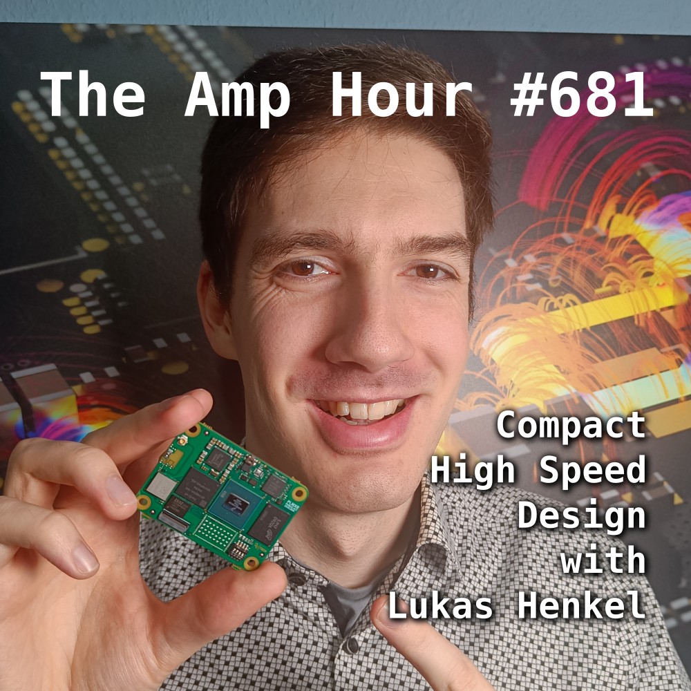
Welcome Lukas Henkel of OV Tech GmbH, a product design firm based in Nuremburg Germany!
- Miniturization and the limits of miniturization
- Price is a constraint
- Using standard PCB tech (off the shelf)
- Open source SIP
- Steps
- Conventional pcbs / components
- Silicon inductors embedded in boards
- Bonded Bare dies / stacked
- Need volume to make it work
- Requirements to fit into ______
- iMX8 ULP – 0.4mm CSP
- SIP Footprint
- Module abstraction layer talk
- Framework laptop
- Software support / BSP
- SIP will be different than PiMX8
- Crowdsupply campaign launching 2-3 weeks and delivery in Dec/Jan
- OpenSource laptop
- CM4 vs PiMX8
- SPI Flash with backup partition
- Secure element SE050
- Footprint for coral tpu and Halo 8
- Trying to solve the problem of vision use cases
- Marketing using layout / products but also making money on it
- Katerina show
- Visualizing simulations
- Developing intuition
- OpenEMS
- Usability is based on python scripting
- Using Blender for heat map
- BVTKNodes uses .vtk file output
- Multiphysics solvers
- Things that drive Lukas
- For HDI, Thinking in 3D / 2.5D and being able to visualize
- Layers ranging from 4 to 18
- Any layer design for SIP
- Wurth electroncis for high density “any layer stackup”
- Article series on altium for the open laptop
- Follow Lukas on LinkedIn
Lukas also was a co-founder of PCB Arts. We had his cofounder Saber on the show in the past.
297 episodes

))